[PDF] ISSI DDR3 SDRAM Layout Guidelines: Master High-Speed PCB Design! High speed pcb design and manufacturing
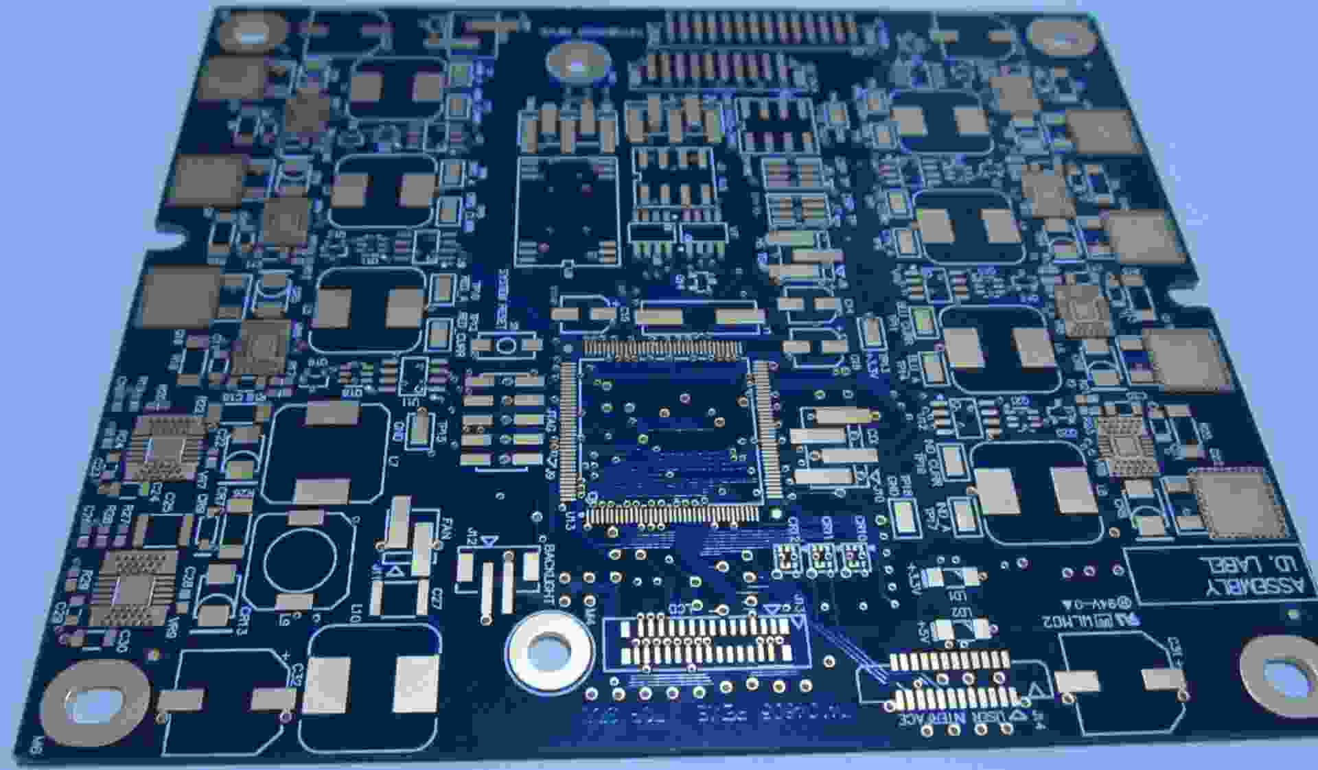
Right, let's talk about PCB design. It's an area where getting the details right can really make or break a project. We're not just slapping components on a board; we're crafting intricate systems where signal integrity and efficient routing are paramount. I've been looking at some examples, and it's fascinating to see the different approaches people take.
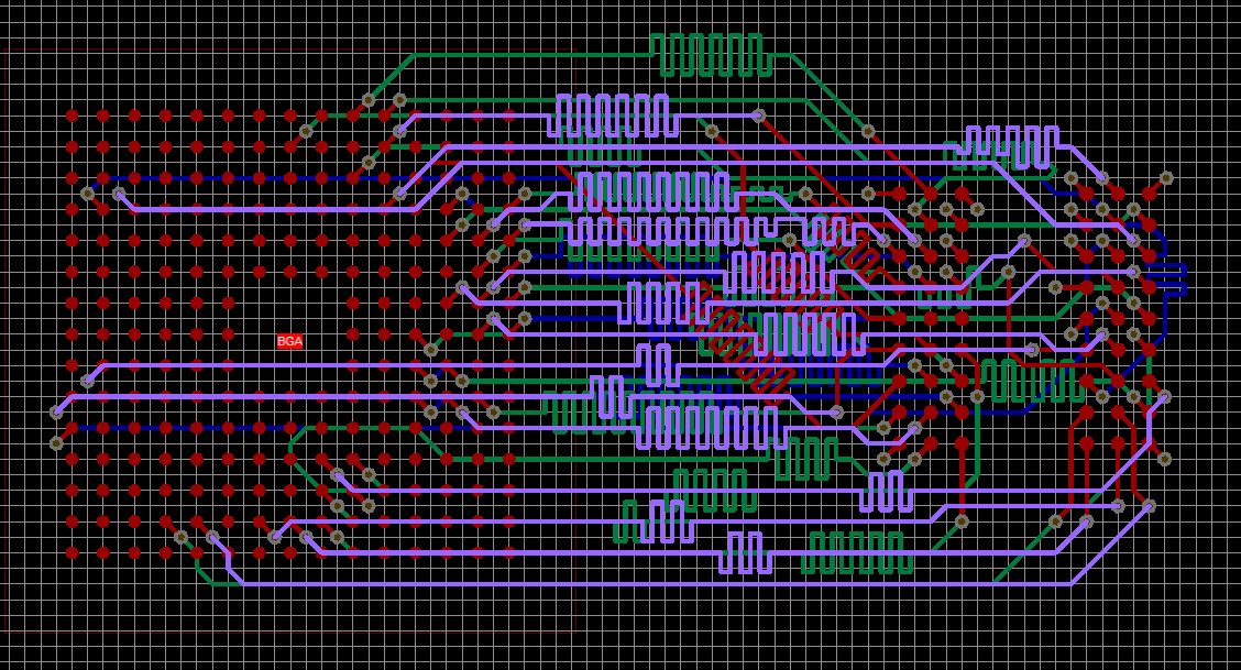
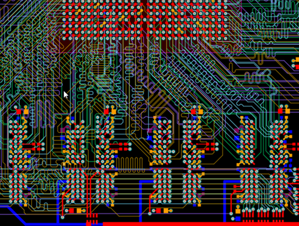
DDR Routing Example
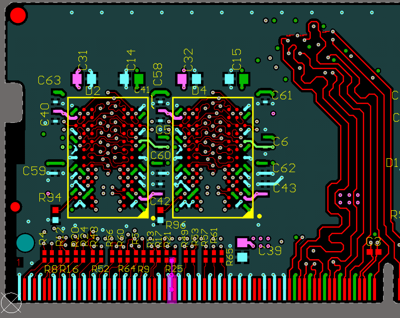
This image showcases DDR routing, and the attention to detail is immediately apparent. Notice how the traces are meticulously routed to minimize impedance discontinuities. This is crucial for maintaining signal integrity in high-speed memory interfaces. The consistent trace widths and controlled impedance lines are essential for preventing signal reflections, which can degrade performance and introduce timing issues. The careful arrangement of the components and the strategic placement of decoupling capacitors are also noteworthy. These capacitors help to filter out noise and provide a stable voltage supply to the memory chips. We're aiming for clean signals, predictable timing, and reliable operation. It's these little things that add up to a robust and high-performing system. The use of ground planes is also very important to minimize signal interference and ensure stable power delivery to the components. The vias, which are used to connect different layers of the board, are carefully placed and sized to minimize signal disruptions. This type of layout requires a high level of expertise and attention to detail, but it's well worth the effort when dealing with high-speed signals.
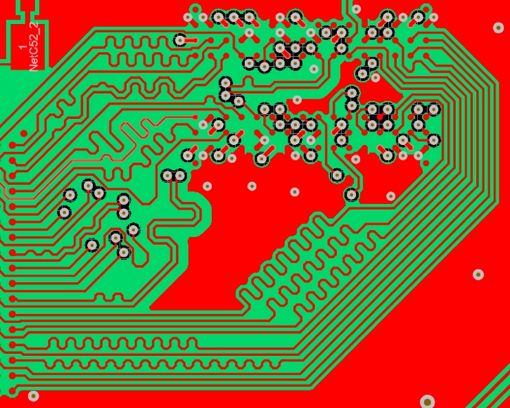
High-Speed Design with Blind Vias and Via-in-Pad Technology

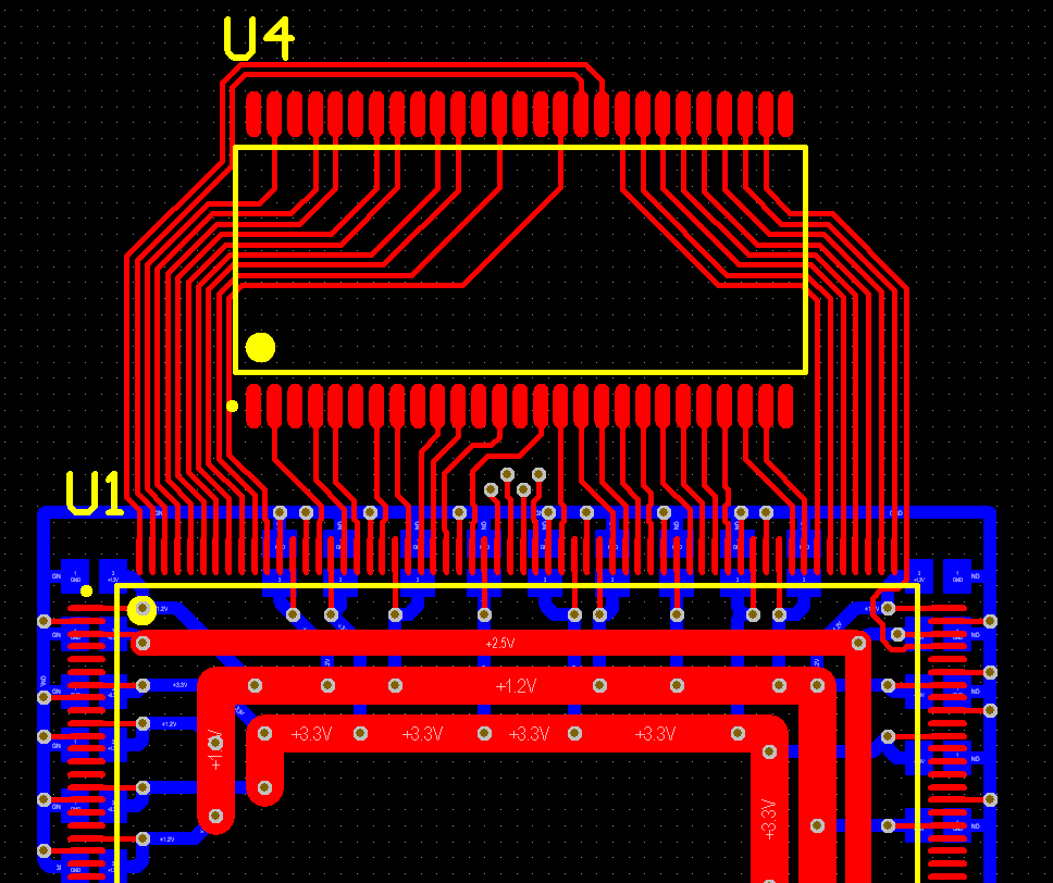
Now, this image delves into the world of high-speed design, specifically with the implementation of blind vias and via-in-pad technology. It is important to note that as signal speeds increase, traditional through-hole vias can introduce significant signal integrity issues due to their stub effect. Blind vias, which connect an outer layer to one or more inner layers, but not all layers, help to minimize this stub effect and reduce signal reflections. Via-in-pad technology takes this even further by placing the vias directly within the component pads, thereby minimizing trace lengths and further improving signal integrity. This is particularly critical for dense boards with fine-pitch components. Look at the density achieved here! The careful placement of components, the short trace lengths, and the use of advanced via technologies all contribute to a high-performance design capable of handling data rates of 6 Gbps. Additionally, the power and ground planes are designed to provide a stable voltage supply and minimize ground bounce, which is crucial for preventing noise and ensuring reliable operation. The use of simulation tools is also essential to verify the signal integrity and optimize the layout for best performance. This level of sophistication is becoming increasingly necessary as we push the boundaries of what's possible with PCB technology. This type of design demands a deep understanding of signal integrity principles and advanced manufacturing techniques. The precision and accuracy required are immense, but the results speak for themselves. It's a testament to the ingenuity and skill of PCB designers who are constantly pushing the limits of what's achievable.
If you are looking for High Speed Pcb Layout Guidelines - Design Talk you've visit to the right web. We have 25 Pictures about High Speed Pcb Layout Guidelines - Design Talk like Issi ddr3 Layout Guideline | PDF, DDR2 and DDR3 SDRAM Interface Termination and Layout Guidelines | PDF and also Main Design Guidelines & Layout Rules on High Speed PCB. Here you go:
High Speed Pcb Layout Guidelines - Design Talk
 design.udlvirtual.edu.pe
 High Speed PCB Design And Manufacturing | Northwest Engineering Solutions
 www.nwengineeringllc.com
 Issi Ddr3 Layout Guideline | PDF
 www.scribd.com
 High Speed Prototype Pcb Layout Design Printing Assembly Services - Buy
 www.alibaba.com
 Stm32 Sdram Pcb Layout Pcb Artists - Vrogue.co
 www.vrogue.co
 DDR2, DDR3, And DDR4 SDRAM Board Design Guidelines 4 - … / Ddr2-ddr3
 pdf4pro.com
 What Is High Speed PCB Design - Guidelines And Best Practice Tips - IBE
 www.pcbaaa.com
 Mobile DDR SDRAM - ISSI | Mouser
 www.mouser.com
 block diagram functional ddr sdram mouser issi mobile
Main Design Guidelines & Layout Rules On High Speed PCB
 www.integrasources.com
 PCB Factory: High-speed PCB Design Sharing Based On Cadence - Kingford
 www.kingfordpcb.com
 Pcb Design Guidelines Mechanical Layer Eurocircuits Eurocircuits Images
www.tpsearchtool.com High Speed Pcb Design Guidelines - Design Talk
 design.udlvirtual.edu.pe
 An520 DDR3 SDRAM Memory Interface Termination And Layout Guidelines
 www.scribd.com
 High Speed Pcb Layout Guidelines - Design Talk
 design.udlvirtual.edu.pe
 Stm32 Sdram Pcb Layout Pcb Artists - Vrogue.co
 www.vrogue.co
 DDR3 SDRAM Memory Interface Termination And Layout Guidelines - DocsLib
 docslib.org
 IS43/46TR 1-Gbit DDR3 SDRAM With ECC - ISSI | Mouser
 www.mouser.com
 Alpha PCB - PCB Design
alphapcbdesigns.com design pcb pad via pads speed high blind vias gbps technology alpha
Emi Emc Guidelines Pcb Layout Pcb Design Guidline For Emi & Emc
 circuitschematics.z20.web.core.windows.net
 ISSI 8Gb DDR3 SDRAM | New Product Brief - New Products
 www.allaboutcircuits.com
 issi
Using SDRAM Vs. DDR RAM In Your PCB Design | Blog | Altium Designer
 resources.altium.com
 Main Design Guidelines & Layout Rules On High Speed PCB
 www.integrasources.com
 High Speed PCB Design Guidelines: Routing And Layer Stackup Techniques
 www.viasion.com
 DDR2 And DDR3 SDRAM Interface Termination And Layout Guidelines | PDF
 www.scribd.com
 High Speed PCB Design Guidelines: Routing And Layer Stackup Techniques
 www.viasion.com
 Ddr2, ddr3, and ddr4 sdram board design guidelines 4. What is high speed pcb design. Ddr2 and ddr3 sdram interface termination and layout guidelines